Endless Reasons for Upgrading to CADint PCB Software
(click below for more details)
-
SCHEMATIC CAPTURE
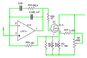
Our Hierarchical Schematic capture is second to none. Unlimited capabilities include multi−bus structure with 99 different bus names, different widths for different buses. You can trace a signal throughout the entire design including systems schematic which contains multiple PCB designs, purchased parts, etc.

-
100% TRUE BI−DIRECTIONAL (BACK AND FORTH) BETWEEN SCHEMATIC and PCB DESIGN
The Schematic Design and PCB Layout Design are parametric. Any changes made to either schematic or layout design is available to update the companion file to reflect any changes.
-
ASCII IMPORTS IN BOTH SCHEMATIC AND PCB DESIGNS
CADint can import ASCII data from several older platforms such as Visula, CADstar, PADS, EEDesigner, P−CAD, Protel, Tango, Edwin, etc.
-
PCB DESIGNS
There is NO limit to the size, shape or layer count (package dependent) CADint PCB when creating PCB designs. The only CADint PCB limitation is your imagination. Packages available include; 2 layer, 4 layer, 6 layer, 10 layer and unlimited layers.
-
AUTOROUTER - CADint PCB designs can be used with a separate interactive autorouter from CADint (Electra Autorouter)
CADint has a separate Autorouter for PCB designs. PCB layouts are exported to the Electra Autorouter, processed, and then imported back into CADint PCB. Contact CADint Sales for information on obtaining the Electra Autorouter software.
-
ONLY CADINT CAN BLOCK/COPY/DROP SCHEMATIC OR LAYOUT FEATURES
Block/Copy/Drop is a way to describe being able to pick ANY section in a schematic and/or design, Copy it and Drop it anywhere you like. These Block copies can be placed within the same schematic/design or placed in a totally different design. Block/Copy/Drop allows you to save a schematic circuit and it’s layout for future use anywhere any time. You can also copy/move anything to any new location within .000001 of an inch.
-
UNLIMITED PLANE CREATION PER LAYER AND PER BOARD
CADint provides a powerful plane generation feature. You can create unlimited copper pours on any layer of your design using CADint. Some of the user−defined plane features included are: Clearance, Outline width, Thermal Connection Width, Thermal Backoff Distance, Board Backoff Distance, Keepout areas, Embed Reference Net Vias, Embed Reference Net Traces. Each plane can be independently named and poured using the Net name of your choice. For example a ground plane can be tied to the ground Net.
-
GERBER DATA GENERATION
CADint offers a one button Gerber and NC drill data generation. You have to see it to believe it. The command is even called “Easy Gerber and Drill”. CADint looks for Gerber and NC data and presents a selection list you pick from to create a fabrication package. It even gives you the option of zipping the data into one file.
CADint allows full generation of individual component Gerbers, similar to the legacy way of generating Gerber files.
CADint includes a fully functional Gerber Viewer. Any generated Gerber file from any software package can be loaded, modified, mirrored and saved for use in CADint PCB.
CADint can generate all panelization Gerber’s, NC drill, and fabrication drawings.
-
FABRICATION AND ASSEMBLY DRAWING GENERATION
CADint allows for the generation of PCB images with superimposed, standard or user generated title blocks for quick generation of any support documentation. There are several stock images but you can create your own on the fly and have them every time you want to create a support document. You can import a DXF image of your title block.
-
DESIGN OUTPUTS AND READABLE COLOR PRINTING
CADint has numerous types of output reporting such as:Bill of Materials, Purchasing list, Excel) along with TIFF, BitMap and Screen Dump. Programmable colors in printing. There are 6 Pick & Place formats (Panasonic, MyData, MyData Old, Siemens, Siemens Svm, SPEA ATOS2 neutral) and Generic formats. ALL of which load directly into Assembly House Pick & Place machines.
-
TECH SUPPORT
CADint’s tech support starts when you down load the free software and continues at no cost as long as you own the package. All you need to do is call us.
We invite you to discover what world−class software and support is really all about. We look forward to hearing from you.You can also send us your files and we can work to help diagnose the issues with or for you. A diagnosis will be emailed to you. NDA’s are supported for intellectual property concerns.
Contact Technical Support either by phone at +1(800)553−1177 or at support@cadint.com.
-
GERBER AND DXF IMPORT
CADint can accept Gerber and DXF data import. CADint can import a DXF file and convert that file to copper. Ideal for reconstructing master layout files from damaged or older files and for converting obsolete PCB CAD packages. In CADint, the time required to re−create a design is significantly reduced since gerber data can be imported as individual files and assigned to what ever layer you want. Once imported, you can select a destination layer, just like third party CAM programs. While this is not an “intelligent” import, it provides an exact placement “roadmap” of the target PCB. base. The actual parts can be positioned directly over the imported gerber data. Traces can be routed using the Gerber data as a pattern. Once the routes are completed, run a DRC & clearance check to verify your work. Once you have completed this step the layout can be recovered and the schematic generated using the recovered layout.
CADint is A Leading Worldwide Supplier of CAD/CAE Software
With offices in The US and Europe we are well poised to offer quality support throughout the world.
System Highlights
- High performance architecture
- Unlimited number of trace widths, pads, hole size
- Unlimited number of via sizes and shapes
- Unlimited number of components per board, etc.
- Simple consistent graphical user interface
- Submicron precision with a resolution of 0.000001m
- Intelligent hierarchical database structure
- Ability to view and edit schematic in layout
- User programmable accelerator keys and tool bar
- Check and view connectivity quickly and accurately
- Any net can be viewed either graphically or in “net list” format
- Clearance violations are easily located and corrected using the View Next command
Post-Processing Features
- One-step generation of photoplotter and drill data, or Unlimited programmable GBR creation… Learn More?
- Powerful plotting module with: Flexible sheet set management for mixing various view on a single sheet
- Output to any Windows printers
- Output to file graphics formats: DXF, Gerber, HPGL, Postscript and more
- Print preview with full pan and zoom
- Pick and Place output in MyData, Panasonic, SPEA Siemens format. Pad/Land/Net/Location Report
- Flexible Bill of Materials and Order List generation loadable directly into Excel
- Test pads/net list generation
- Design note functionality for annotation, drill table, board statistics and other documentation purposes
- Generate all documentation without leaving Cadint by importing customer formats to be used for Fabrication drawings Assembly drawings